lunes, 28 de junio de 2010

Active Versus Passive Devices

Electronic components are classed into either being Passive devices or Active devices. Active devices are different from passive devices. These devices are capable of changing their operational performance, may deliver power to the circuit, and can perform interesting mathematical functions. While a device that does not require a source of energy for its operation.


What are Active Devices?
An active device is any type of circuit component with the ability to electrically control electron flow (electricity controlling electricity). In order for a circuit to be properly called electronic, it must contain at least one active device. Active devices include, but are not limited to, vacuum tubes, transistors, silicon-controlled rectifiers (SCRs), and TRIACs.

All active devices control the flow of electrons through them. Some active devices allow a voltage to control this current while other active devices allow another current to do the job. Devices utilizing a static voltage as the controlling signal are, not surprisingly, called voltage-controlled devices. Devices working on the principle of one current controlling another current are known as current-controlled devices. For the record, vacuum tubes are voltage-controlled devices while transistors are made as either voltage-controlled or current controlled types. The first type of transistor successfully demonstrated was a current-controlled device.

What are Passive Devices?
Components incapable of controlling current by means of another electrical signal are called passive devices. Resistors, capacitors, inductors, transformers, and even diodes are all considered passive devices.

Passive devices are the resistors, capacitors, and inductors required to build electronic hardware. They always have a gain less than one, thus they can not oscillate or amplify a signal. A combination of passive components can multiply a signal by values less than one, they can shift the phase of a signal, they can reject a signal because it is not made up of the correct frequencies, they can control complex circuits, but they can not multiply by more than one because they lack gain.

Diodes
Diodes are basically a one-way valve for electrical current. They let it flow in one direction (from positive to negative) and not in the other direction. Most diodes are similar in appearance to a resistor and will have a painted line on one end showing the direction or flow (white side is negative). If the negative side is on the negative end of the circuit, current will flow. If the negative is on the positive side of the circuit no current will flow. More on diodes in later sections.
Integrated Circuits
Integrated Circuits, or ICs, are complex circuits inside one simple package. Silicon and metals are used to simulate resistors, capacitors, transistors, etc. It is a space saving miracle. These components come in a wide variety of packages and sizes. You can tell them by their "monolithic shape" that has a ton of "pins" coming out of them. Their applications are as varied as their packages. It can be a simple timer, to a complex logic circuit, or even a microcontroller (microprocessor with a few added functions) with erasable memory built inside.

Transistors
A transistor is a semiconductor device, commonly used as an amplifier or an electrically controlled switch. The transistor is the fundamental building block of the circuitry in computers, cellular phones, and all other modern electronic devices.

Because of its fast response and accuracy, the transistor is used in a wide variety of digital and analog functions, including amplification, switching, voltage regulation, signal modulation, and oscillators. Transistors may be packaged individually or as part of an integrated circuit, some with over a billion transistors in a very small area - part of a trend of increasing transistor density known as Moore's Law.

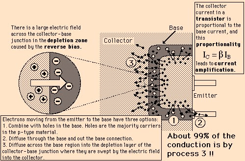
Transistor stands for transit resistor, the temporary name, now permanent, that the inventors gave it. These semidconductors control the electrical current flowing between two terminals by applying voltage to a third terminal. You now have a minature switch, presenting either a freeway to electrons or a brick wall to them, depending on whether a signal voltage exists. Bulky mechanical relays that used to switch calls, like the crossbar shown above, could now be replaced with transistors. There's more.

Transistors amplify when built into a proper circuit. A weak signal can be boosted tremendously. Let's say you have ten watts flowing into one side of the transistor. Your current stops because silicon normally isn't a good conductor. You now introduce a signal into the middle of the transistor, say, at one watt. That changes the transistor's internal crystalline structure, causing the silicon to go from an insulator to a conductor. It now allows the larger current to go through, picking up your weak signal along the way, impressing it on the larger voltage. Your one watt signal is now a ten watt signal.

Transistors use the properties of semi-conductors, seemingly innocuous materials like geranium and now mostly silicon. Materials like silver and copper conduct electricity well. Rubber and porcelain conduct electricity poorly. The difference between electrical conductors and insulators is their molecular structure, the stuff that makes them up. Weight, size, or shape doesn't matter, it's how tightly the material holds on to its electrons, preventing them from freely flowing through its atoms.
First Transistor

Active Versus Passive Devices in the News
Seven Steps to Successful Analog-to-Digital Signal Conversion
Understand how to balance gain blocks and noise, and perform noise calculations for proper signal conditioning Signal processing - Business - Technology - Electronics - Integrated circuit

Class D Speaker Amplifier offers automatic level control.
Designed for battery-operated portable devices, 2.2 W MAX98500 integrates boost converter to provide constant output power. Class D amplifier is equipped with battery-tracking Automatic Level Control circuit that limits max output swing as supply voltage drops. ALC helps to avoid clipping and prevents battery voltage from collapsing. Housed in 2.1 x 2.1 mm WLP, MAX98500 accepts 2.5-5.5 V supply ...

Rohde & Schwarz find scope for expansion

Rohde & Schwarz is today launching its first dedicated oscilloscopes. It has developed its own ASICs and A to D converters to support the new design which is described as 20 times faster than existing devices. Oscilloscope - Technology - Theory of Measurements - Electronics - Integrated circuit

TRANSISTOR SPECIFICATIONS

Transistors are available in a large variety of shapes and sizes, each with its own unique characteristics. The characteristics for each of these transistors are usually presented on SPECIFICATION SHEETS or they may be included in transistor manuals. Although many properties of a transistor could be specified on these sheets, manufacturers list only some of them. The specifications listed vary with different manufacturers, the type of transistor, and the application of the transistor. The specifications usually cover the following items.

A general description of the transistor that includes the following information:

The kind of transistor. This covers the material used, such as germanium or silicon; the type of transistor(NPN or PNP); and the construction of the transistor(whether alloy-junction, grown, or diffused junction, etc.).
Some of the common applications for the transistor, such as audio amplifier, oscillator, rf amplifier, etc.
General sales features, such as size and packaging(mechanical data).
The "Absolute Maximum Ratings" of the transistor are the direct voltage and current values that if exceeded in operation may result in transistor failure. Maximum ratings usually include collector-to-base voltage, emitter-to-base voltage, collector current, emitter current, and collector power dissipation. The typical operating values of the transistor. These values are presented only as a guide. The values vary widely, are dependent upon operating voltages, and also upon which element is common in the circuit. The values listed may include collector-emitter voltage, collector current, input resistance, load resistance, current-transfer ratio(another name for alpha or beta), and collector cutoff current, which is leakage current from collector to base when no emitter current is applied. Transistor characteristic curves may also be included in this section. A transistor characteristic curve is a graph plotting the relationship between currents and voltages in a circuit. More than one curve on a graph is called a "family of curves." Additional information for engineering-design purposes.

TRANSISTOR IDENTIFICATION

Transistors can be identified by a Joint Army-Navy (JAN) designation printed directly on the case of the transistor. The marking scheme explained earlier for diodes is also used for transistor identification. The first number indicates the number of junctions. The letter "N" following the first number tells us that the component is a semiconductor. And, the 2- or 3-digit number following the N is the manufacturer's identification number. If the last number is followed by a letter, it indicates a later, improved version of the device. For example, a semiconductor designated as type 2N130A signifies a three-element transistor of semiconductor material that is an improved version of type 130:

You may also find other markings on transistors that do not relate to the JAN marking system. These markings are manufacturers' identifications and may not conform to a standardized system. If in doubt, always replace a transistor with one having identical markings. To ensure that an identical replacement or a correct substitute is used, consult an equipment or transistor manual for specifications on the transistor.

TRANSISTOR MAINTENANCE

Transistors are very rugged and are expected to be relatively trouble free. Encapsulation and conformal coating techniques now in use promise extremely long life expectancies. In theory, a transistor should last indefinitely. However, if transistors are subjected to current overloads, the junctions will be damaged or even destroyed. In addition, the application of excessively high operating voltages can damage or destroy the junctions through arc-over or excessive reverse currents. One of the greatest dangers to the transistor is heat, which will cause excessive current flow and eventual destruction of the transistor.

To determine if a transistor is good or bad, you can check it with an ohmmeter or a transistor tester. In many cases, you can substitute a transistor known to be good for one that is questionable and thus determine the condition of a suspected transistor. This method of testing is highly accurate and sometimes the quickest, but it should be used only after you make certain that there are no circuit defects that might damage the replacement transistor. If more than one defective transistor is present in the equipment where the trouble has been localized, this testing method becomes cumbersome, as several transistors may have to be replaced before the trouble is corrected. To determine which stages failed and which transistors are not defective, all the removed transistors must be tested. This test can be made by using a standard Navy ohmmeter, transistor tester, or by observing whether the equipment operates correctly as each of the removed transistors is reinserted into the equipment. A word of caution-indiscriminate substitution of transistors in critical circuits should be avoided.

The History of the Integrated Circuit

Our world is full of integrated circuits. You find several of them in computers. For example, most people have probably heard about the microprocessor. The microprocessor is an integrated circuit that processes all information in the computer. It keeps track of what keys are pressed and if the mouse has been moved. It counts numbers and runs programs, games and the operating system. Integrated circuits are also found in almost every modern electrical device such as cars, television sets, CD players, cellular phones, etc. But what is an integrated circuit and what is the history behind it?


Electric Circuits

The integrated circuit is nothing more than a very advanced electric circuit. An electric circuit is made from different electrical components such as transistors, resistors, capacitors and diodes, that are connected to each other in different ways. These components have different behaviors.

The transistor acts like a switch. It can turn electricity on or off, or it can amplify current. It is used for example in computers to store information, or in stereo amplifiers to make the sound signal stronger.

The resistor limits the flow of electricity and gives us the possibility to control the amount of current that is allowed to pass. Resistors are used, among other things, to control the volume in television sets or radios.

The capacitor collects electricity and releases it all in one quick burst; like for instance in cameras where a tiny battery can provide enough energy to fire the flashbulb.

The diode stops electricity under some conditions and allows it to pass only when these conditions change. This is used in, for example, photocells where a light beam that is broken triggers the diode to stop electricity from flowing through it.

These components are like the building blocks in an electrical construction kit. Depending on how the components are put together when building the circuit, everything from a burglar alarm to a computer microprocessor can be constructed.

The Transistor vs. the Vacuum Tube

Of the components mentioned above, the transistor is the most important one for the development of modern computers. Before the transistor, engineers had to use vacuum tubes. Just as the transistor, the vacuum tube can switch electricity on or off, or amplify a current. So why was the vacuum tube replaced by the transistor? There are several reasons.

The vacuum tube looks and behaves very much like a light bulb; it generates a lot of heat and has a tendency to burn out. Also, compared to the transistor it is slow, big and bulky


When engineers tried to build complex circuits using the vacuum tube, they quickly became aware of its limitations. The first digital computer ENIAC, for example, was a huge monster that weighed over thirty tons, and consumed 200 kilowatts of electrical power. It had around 18,000 vacuum tubes that constantly burned out, making it very unreliable.

When the transistor was invented in 1947 it was considered a revolution. Small, fast, reliable and effective, it quickly replaced the vacuum tube. Freed from the limitations of the vacuum tube, engineers finally could begin to realize the electrical constructions of their dreams, or could they?


The Tyranny of Numbers

With the small and effective transistor at their hands, electrical engineers of the 50s saw the possibilities of constructing far more advanced circuits than before. However, as the complexity of the circuits grew, problems started arising.

When building a circuit, it is very important that all connections are intact. If not, the electrical current will be stopped on its way through the circuit, making the circuit fail. Before the integrated circuit, assembly workers had to construct circuits by hand, soldering each component in place and connecting them with metal wires. Engineers soon realized that manually assembling the vast number of tiny components needed in, for example, a computer would be impossible, especially without generating a single faulty connection.

Another problem was the size of the circuits. A complex circuit, like a computer, was dependent on speed. If the components of the computer were too large or the wires interconnecting them too long, the electric signals couldn't travel fast enough through the circuit, thus making the computer too slow to be effective.

So there was a problem of numbers. Advanced circuits contained so many components and connections that they were virtually impossible to build. This problem was known as the tyranny of numbers.

Jack Kilby's Chip - the Monolithic Idea


In the summer of 1958 Jack Kilby at Texas Instruments found a solution to this problem. He was newly employed and had been set to work on a project to build smaller electrical circuits. However, the path that Texas Instruments had chosen for its miniaturization project didn't seem to be the right one to Kilby.

Because he was newly employed, Kilby had no vacation like the rest of the staff. Working alone in the lab, he saw an opportunity to find a solution of his own to the miniaturization problem. Kilby's idea was to make all the components and the chip out of the same block (monolith) of semiconductor material. When the rest of the workers returned from vacation, Kilby presented his new idea to his superiors. He was allowed to build a test version of his circuit. In September 1958, he had his first integrated circuit ready. It was tested and it worked perfectly!

Although the first integrated circuit was pretty crude and had some problems, the idea was groundbreaking. By making all the parts out of the same block of material and adding the metal needed to connect them as a layer on top of it, there was no more need for individual discrete components. No more wires and components had to be assembled manually. The circuits could be made smaller and the manufacturing process could be automated.

Jack Kilby is probably most famous for his invention of the integrated circuit, for which he received the Nobel Prize in Physics in the year 2000. After his success with the integrated circuit Kilby stayed with Texas Instruments and, among other things, he led the team that invented the hand-held calculator.

Robert Noyce

Robert Noyce came up with his own idea for the integrated circuit. He did it half a year later than Jack Kilby. Noyce's circuit solved several practical problems that Kilby's circuit had, mainly the problem of interconnecting all the components on the chip. This was done by adding the metal as a final layer and then removing some of it so that the wires needed to connect the components were formed. This made the integrated circuit more suitable for mass production. Besides being one of the early pioneers of the integrated circuit, Robert Noyce also was one of the co-founders of Intel. Intel is one of the largest manufacturers of integrated circuits in the world.

Chip Production Today - in Short

Chip production today is based on photolithography. In photolithography a high energy UV-light is shone through a mask onto a slice of silicon covered with a photosensitive film. The mask describes the parts of the chip and the UV-light will only hit the areas not covered by the mask. When the film is developed, the areas hit by light are removed. Now the chip has unprotected and protected areas forming a pattern that is the first step to the final components of the chip.

Next, the unprotected areas are processed so their electrical properties change. A new layer of material is added, and the entire process is then repeated to build the circuit, layer by layer. When all the components have been made and the circuit is complete a layer of metal is added. Just as before, a layer of photosensitive film is applied and exposed through a mask. However, this time the mask used describes the layout of the wires connecting all the parts of the chip. The film is developed and the unexposed parts are removed. Next, the metal not protected with film is removed to form the wires. Finally, the chip is tested and packaged.

When making chips today, a process called "stepping" is often used. On a big wafer of silicon the chips are made one next to the other. The silicon wafer is moved in steps under the mask and the UV-light to expose the wafer. In this way, chip after chip can be made using the same mask each time.

Below is a more sequential description of the process of making a modern integrated circuit. But let us first take a look at the special place where integrated circuits are produced - the clean room.

The Clean Room

The sizes of the components on chips produced in a modern chip fabrication plant are extremely small. For a better understanding of how small they are, pick a hair from your head and cut it in half. Now look at the cross section. On this tiny area, hard to see with the bare eye, you can fit thousands of modern transistors.

With sizes this small, the production of a chip demands precision at an atomic level. Tiny particles like a hair, a speck of dust, a dead skin cell, bacteria or even the single particles in tobacco smoke become huge objects that are big enough to ruin a chip.

Therefore, chip production takes place in a clean room. This is a specially designed room, where furniture is built from special materials that don't give off particles, and where extremely effective air filters and air circulation systems change the air completely up to ten times a minute.

To further prevent contamination, workers wear special suits called "bunny suits." These protective outfits are made of ultra clean material and sometimes have their own air filtering systems.

Chip Production Today - in Detail

Building an integrated circuit like a computer chip is a very complex process. It is divided into two major parts, front end and back end. In the front end, you make the components of the circuit. In the back end, you add metal to connect the components and then you test and package the chip. Below is a simplified description of the steps.

Breakdown voltage

The breakdown voltage of an Insulator is the minimum voltage that causes a portion of an insulator to become electrically conductive.
The breakdown voltage of a diode is the minimum reverse voltage to make the diode conduct in reverse. Some devices (such as TRIACs) also have a forward breakdown voltage.

High voltage dielectric breakdown within a block of plexiglas

In Detail

Insulators
Breakdown voltage is a characteristic of an insulator that defines the maximum voltage difference that can be applied across the material before the insulator collapses and conducts. In solid insulating materials, this usually creates a weakened path within the material by creating permanent molecular or physical changes by the sudden current. Within rarefied gases found in certain types of lamps, breakdown voltage is also sometimes called the "striking voltage".[2]
The breakdown voltage of a material is not a definite value because it is a form of failure and there is a statistical probability whether the material will fail at a given voltage. When a value is given it is usually the mean breakdown voltage of a large sample. Another term is also 'withstand voltage' where the probability of failure at a given voltage is so low it is considered, when designing insulation, that the material will not fail at this voltage.[3]
Two different breakdown voltage measurements of a material are the AC and impulse breakdown voltages. The AC voltage is the line frequency of the mains (either 50 or 60 Hz depending on where you live). The impulse breakdown voltage is simulating lightning strikes, and usually uses a 1.2 microsecond rise for the wave to reach 90% amplitude then drops back down to 50% amplitude after 50 microseconds.[4]
Two technical standards governing performing these tests are ASTM D1816 and ASTM D3300 published by ASTM.

Breakdown in vacuum
In standard conditions at atmospheric pressure, gas serves as an excellent insulator, requiring the application of a significant voltage before breaking down (e.g. lightning). In partial vacuum, this breakdown potential may decrease to an extent that two uninsulated surfaces with different potentials might induce the electrical breakdown of the surrounding gas. This has some useful applications in industry (e.g. the production of microprocessors) but in other situations may damage an apparatus, as breakdown is analogous to a short circuit.

The breakdown voltage in a partial vacuum is represented as


where Vb is the breakdown potential in volts DC, A and B are constants that depend on the surrounding gas, p represents the pressure of the surrounding gas, d represents the distance in centimetres between the electrodes, and γse represents the Secondary Electron Emission Coefficient.

Diodes
Breakdown voltage is a parameter of a diode that defines the largest reverse voltage that can be applied without causing an exponential increase in the current in the diode. As long as the current is limited, exceeding the breakdown voltage of a diode does no harm to the diode. In fact, Zener diodes are essentially just heavily doped normal diodes that exploit the breakdown voltage of a diode to provide regulation of voltage levels.
iode I-V diagram

Avalanche Breakdown
Avalanche Breakdown in Germanium
It is shown that all germanium junctions studied break down as the result of the same avalanche process found in silicon. An empirical expression for the multiplication inherent in this breakdown process is given for step junctions. Ionization rates for holes and electrons in Ge are derived with the use of this expression. The ionization rate for holes is larger than that for electrons by about a factor of two. The agreement between these ionization rates as a function of field and the theory of Wolff is excellent. It is determined that the threshold for electron-hole pair production is about 1.50 ev and the mean free path for electron (or hole)-phonon collisions is about 130 A.

Low-voltage organic transistors with an amorphous molecular gate dielectric
Organic thin film transistors (TFTs) are of interest for a variety of large-area electronic applications, such as displays1, 2, 3, sensors and electronic barcodes. One of the key problems with existing organic TFTs is their large operating voltage, which often exceeds 20 V. This is due to poor capacitive coupling through relatively thick gate dielectric layers: these dielectrics are usually either inorganic oxides or nitrides2, 3, 4, 5, 6, 7, 8, or insulating polymers9, and are often thicker than 100 nm to minimize gate leakage currents. Here we demonstrate a manufacturing process for TFTs with a 2.5-nm-thick molecular self-assembled monolayer (SAM) gate dielectric and a high-mobility organic semiconductor (pentacene). These TFTs operate with supply voltages of less than 2 V, yet have gate currents that are lower than those of advanced silicon field-effect transistors with SiO2 dielectrics. These results should therefore increase the prospects of using organic TFTs in low-power applications (such as portable devices). Moreover, molecular SAMs may even be of interest for advanced silicon transistors where the continued reduction in dielectric thickness leads to ever greater gate leakage and power dissipation.

A new drain-current injection technique for the measurement of off-state breakdown voltage in FET's
We present a new simple three-terminal technique to measure the off-state breakdown voltage of FET's. With the source grounded, current is injected into the drain of the on-state device. The gate is then ramped down to shut the device off. In this process, the drain-source voltage rises to a peak and then drops. This peak represents an unambiguous definition of three-terminal breakdown voltage. In the same scan, we additionally obtain a measurement of the two-terminal gate-drain breakdown voltage. The proposed method offers potential for use in a manufacturing environment, as it is fully automatable. It also enables easy measurement of breakdown voltage in unstable and fragile devices

domingo, 20 de junio de 2010

Chapter Summary

-The bipolar junction transistor (BJT) was invented in the late 1940s at the Bell Telephone Laboratories by Bardeen, Brattain, and Shockley and became the first commercially successful three-terminal solid-state device.
-Although the FET has become the dominant device technology in modern integrated circuits, bipolar transistors are still widely used in both discrete and integrated circuit design. In particular, the BJT is still the preferred device in many applications that require high speed and/or high precision such as op-amps, A/D and D/A converters, and wireless communication products.
-The basic physical structure of the BJT consists of a three-layer sandwich of alternating p- and n-type semiconductor materials and can be fabricated in either npn or pnp form.
-The emitter of the transistor injects carriers into the base. Most of these carriers traverse the base region and are collected by the collector. The carriers that do not completely traverse the base region give rise to a small current in the base terminal.
-A mathematical model called the transport model (a simplified Gummel-Poon model) characterizes the i-v characteristics of the bipolar transistor for general terminal voltage and current conditions. The transport model requires three unique parameters to characterize a particular BJT: the saturation current IS and the forward and reverse common-emitter current gains βF and βR.
-βF is a relatively large number, ranging from 20 to 500, and characterizes the significant current amplification capability of the BJT. Practical fabrication limitations cause the bipolar transistor structure to be inherently asymmetric, and the value of βR is much smaller than βF, typically between 0 and 2.
-The classical Ebers-Moll model can be obtained from a rearrangement of the transport model equations.
-SPICE circuit analysis programs contain a comprehensive built-in model for the transistor that is an extension of the transport model.
-Four regions of operation -- cutoff, forward-active, reverse-active, and saturation -- were identified for the BJT based on the bias voltages applied to the base-emitter and base-collector junctions. The transport model can be simplified for each individual region of operation.
-The cutoff and saturation regions are most often used in switching applications and logic circuits. In cutoff, the transistor approximates an open switch, whereas in saturation, the transistor represents a closed switch. However, in contrast to the "on" MOSFET, the saturated bipolar transistor has a small voltage, the collector-emitter saturation voltage VCESAT, between its collector and emitter terminals, even when operating with zero collector current.
-In the forward-active region, the bipolar transistor can provide high voltage and current gain for amplification of analog signals. The reverse-active region finds limited use in some analog- and digital-switching applications.
-The i-v characteristics of the bipolar transistor are often presented graphically in the form of the output characteristics, iC versus vCE or vCB, and the transfer characteristics, iC versus vBE or vEB.
-The transconductance gm of the bipolar transistor in the forward-active region relates differential changes in collector current and base-emitter voltage and was shown to be directly proportional to the dc collector current IC.
-In the forward-active region, the collector current increases slightly as the collector-emitter voltage increases. The origin of this effect is base-width modulation, known as the Early effect, and it can be included in the model for the forward-active region through addition of the parameter called the Early voltage VA.
-The collector current of the bipolar transistor is determined by minority-carrier diffusion across the base of the transistor, and expressions were developed that relate the saturation current and base transit time of the transistor to physical device parameters. The base width plays a crucial role in determining the base transit time and the high-frequency operating limits of the transistor.
-Minority-carrier charge is stored in the base of the transistor during its operation, and changes in this stored charge with applied voltage result in diffusion capacitances being associated with forward-biased junctions. The value of the diffusion capacitance is proportional to the collector current IC.
-The capacitances of the bipolar transistor cause the current gain to be frequency-dependent. At the beta cutoff frequency fβ, the current gain has fallen to 71 percent of its low frequency value, whereas the value of the current gain is only 1 at the unity-gain frequency fT.
-A number of biasing circuits were analyzed to determine the Q-point of the transistor. Design of the four-resistor network was investigated in detail. The four-resistor bias circuit provides highly stable control of the operating point and is the most important bias circuit for discrete design.
-The current mirror circuit, which is extremely important for biasing integrated circuits, relies on the use of closely matched transistors for proper operation.
-Techniques for analyzing the influence of element tolerances on circuit performance include the worst-case analysis and statistical Monte Carlo analysis methods. In worst-case analysis, element values are simultaneously pushed to their extremes, and the resulting predictions of circuit behavior are often overly pessimistic. The Monte Carlo method analyzes a large number of randomly selected versions of a circuit to build up a realistic estimate of the statistical distribution of circuit performance. Random number generators in high-level computer languages, spreadsheets, or MATLAB can be used to randomly select element values for use in the Monte Carlo analysis. Some circuit analysis packages such as PSPICE provide a Monte Carlo analysis option as part of the program.


Transistor Operation

A transistor in a circuit will be in one of three conditions
Cut off (no collector current), useful for switch operation.
In the active region (some collector current, more than a few tenths of a volt above the emitter), useful for amplifier applications
In saturation (collector a few tenths of a volt above emitter), large current useful for "switch on" applications.

Collector Current Determination

The base-emitter voltage can be considered to be the controlling variable in determining transistor action. The collector current is related to this voltage by the Ebers-Moll relationship (sometimes labeled the Shockley equation):

The saturation current is characteristic of the particular transistor (a parameter which itself has a temperature dependence). This relationship is stable over a wide range of voltages and currents. A further useful relationship is

where ß can be called the current gain. The value of ß is not highly dependable since it depends on Ic , Vce and the temperature.


Base-Emitter Junction Details

Some useful "rules of thumb" which help in understanding transistor action are (from Horowitz & Hill):
1.- A base emitter voltage Vbe of about 0.6 v will "turn on" the base-emitter diode and that voltage changes very little, < +/- 0.1v throughout the active range of the transistor which may change base current by a factor of 10 or more.
2.- An increase in base-emitter voltage Vbe by about 60 mV will increase the collector current Ic by about a factor of 10.
3.- The effective AC series resistance of the emitter is about 25/ ohms.
4.- The base-emitter voltage is temperature dependent, decreasing about 2.1 mV/C
5.- The base-emitter voltage varies slightly with the collector-emitter voltage at constant collector current : Ic=∆Vbe=-0.01∆Vce

Transistor Action


More about transistor regions

Collector Current

Normal transistor action results in a collector-to-emitter current which is about 99% of the total current. The usual symbols used to express the transistor current relationships are shown.

The proportionality β can take values in the range 20 to 200 and is not a constant even for a given transistor. It increases for larger emitter currents because the larger number of electrons injected into the base exceeds the available holes for recombination so the fraction which recombine to produce base current delines even further.

Use of the Current Gain

Any circuit that depends on a specific value of the current gain is a bad circuit because that value varies for a given transistor as well as between different transistors of the same type.


Modeling of Integrated Circuit Defect Sensitivities

Pinhole defects

One class of defects, known as pinholes, occurs in dielectric insulators such as thin and thick silicon oxides, oxidized poly silicon, chemical vapor deposited insulators, quartz, etc.
These defects are usually much smaller than a micrometer.
Their occurrence can result in a short circuit between conductors produced at different photolithographic levels.
The area in which such defects cause failures is the overlap region between two conductors that cross each other, as shown in Fig. 1. Defects that fall outside these overlap areas cannot cause short circuits. We call the overlap where failures do occur the “critical area.” The words “defect sensitive area” and “susceptible area” have also been used in the same context.
Critical areas of pinholes in most designs can be determined readily as the total overlap area between patterns at different photolithographic levels. When the integrated circuit masks are generated with a computer, algorithms are often available to determine this area fo r an entire chip. The result must be less than the total chip area. Let 0 be the fraction of chip area A that is sensitive to pinholes. The critical area Ac can then be expressed as
Ac = 0A.
The average number of failures or faults caused by the defects can now be calculated by
X = AcD
= θADc
Where D is the density of defects per unit area. This is the direct relationship between defect densities and the average number of faults that also was discussed in previous papers
Some investigations into the defect densities of dielectric pinholes have shown that the average numbeorf failures per monitor can be proportional to the monitor length [4]. A typical structure where this can occur is shown in the cross section of a charge-coupled device in Fig. 2. Stress effects between the two polysilicon patterns create defects a long the edges of the overlap area.
To model these effects one has to count the number of faults that occur along an overlap section of length L. It is then possible to define
X = LD,
Where DL is the density in defects per unit length. This is a model that differs significantly from the area model, since the defect densities are in different units. Yet, if both the area and the length pinhole effects take place in the same chip, their combined number of faults is given by
550 X = AcD + LD,
This result demonstrates an important principle in yield modeling: Faults caused by different failure mechanisms can be added, but defect densities for different failure mechanisms cannot be added. In this example the defect densities have to be modified by both the critical area and the critical length to become faults.
It is possible at this point to expose a myth that seems to recur constantly in yield models used by the semiconductor industry. This myth assumes that the yield can be modeled with only one critical area and one defect density, regardless of the process complexity. Even though thus far we have discussed only one defect type, namely, pinholes, we already see that such an averaging process is impossible. It should be clear that the introduction of other defect types should make this simplification even less likely. The only simplification possible is the use of the cumulative average number of faults X to which all these defects contribute.

Pinhole defect monitors

The relationship between the average number of faults for area pinholes and the defect density D is a simple proportionality.
This simplicity has a useful application. If we have a process without a linear pinhole problem, we can make defect monitors that consist only of a large overlap area between two conductors. By measuring the resistance between the conductors, we can determine when the monitors are short circuited and fail due to pinholes.
Let us assume that we have made N of these monitors and we find that U of these are short-circuited. The monitor yield Y, is then given by
Ym= (N-U)/N
We now want to estimate the average number of faults that cause these failures. Unfortunately, we have no way of knowing how many faults cause a monitor to fail. In most cases it is only one fault, but there canb e instances in which two or more defects cause two or more faults. If the defect density is constant in the sample and the defects occur at random, then the distribution of the number of faults per monitor is given by a Poisson distribution

Photolithographic defects
Patterns of polysilicon, metal, dielectric insulators, and diffusions in silicon wafer surfaces are used to make and interconnect the transistors, diodes, resistors, and capacitors in integrated circuit chips. Minimum pattern dimensions of a few micrometers are typical for the integrated circuits manufactured today. Dust and dirt particles with similar dimensions, or larger, are the major cause of defects in integrated circuit production. Such particles interfere with the photolithographic processes used to define the patterns. Whether a particle causes a failure depends on its location on a chip or on the photographic misused in the process. The size of the resulting defect also determines whether the chip will fail. In many cases small defects don ot cause chip failures a t all.
A theory for mathematically modeling the size dependency of defects was originally developed by R. H. Dennard and P.C o ok at the IBM ThomaJs. Watson Research Center, Yorktown Heights, New York, in the late 1960s. This theory has subsequently been adapted by Madder et al. in a yield model used for manufacturing control. Other yield models that make use of this approach have since been applied for yield projection and line control at a number of IBM manufacturing locations. However, until now only a cursory description of the defect size model has been given in the literature. It is the purpose of the next sections to describe them odel and derive it from fundamental principles.
Critical areas of very long conductors
The effect of defect size on integrated circuit patterns is best approached by first considering a very long straight conductive line. We assume that this conductor is deposited on an insulator and has a length L which is much greater than its width w. This conductive line has to allow an electric current to flow from one end to the other. The failures this case is open circuits caused by holes in the conductive material.
These holes are referred to as missing photolithographic patterns.
It must be pointed out here that there is a class of open circuits that is caused by minute cracks in the conductive material. This usually occurs where the conductor passes over steps from the edges of the patterns underneath. Such defects can be modeled by counting the number of critical steps in a design. This propensity of steps to cause discontinuities can be measured with defect monitors. These defects are not included in the analysis which follows.
When photolithographic defects are very small, there can be enough conductive material left to allow the line to conduct currents without failure. Such a condition is depicted in Fig. 3. We define the defect size as a maximum defect dimension perpendicular to the line edges.

The width of the defect in the longitudinal or horizontal dimension does not matter. In actual cases it is usually of the same magnitude as the universe dimension. It has therefore proven convenient to model the defects as circles, as is done in the rest of this paper. The diameter of each circular defect is designated with the Greek letterx.
The object of our model is to find the mathematical relationship between the critical area and the desfeizcet. We have already seen that for small enough defects the conductor will not fail. We now must consider the maximum amount of conductive material that can be left by a defect and have it still cause a failure. If more than this amount is left, the line will not fail. When less than this amount remains, the line will always fail.
The amount to f the conductor that has left by a defect in order not to cause a failure during final test depends on the electrical current that flows through the line when it is tested.
In this paper we focus attention on models for final test or functional yield of chips. Reliability failures caused by the phenomenon of aluminum migration can be modeled with a similar model but are not treated in this paper. We assume that, during normal operation and final test, the conductor carries enough current to make it "blow" when only a width d of material is left. If the width is greater than d, we assume that the line is not affected, while any amount of material of width d or less always causes a failure.
Thus defects of size x < (w - d) leave enough conductive material to keep the conductor operational, and defects of size x 2 (w - d) cause the line to fail if they occur in the right location. These conditions are known as the failure criteria. The locus of the center of defects that lead to failure is known as the critical area. The critical area is therefore defined as the area in which the center of a defect must fall to cause a failure or a fault.
Let us first determine the critical area for a defect of size
x = (w - d). This area is indicated by the dashed lines in Fig. 4. If the center of the defect falls above the upper dashed line, no failure will occur. Similarly, if the defect is centered below the lower dashed line, there will be no fault. In both these cases more than a width d of conductive material is left.
With the drawing in Fig. 4 we can determine the distance between either edge of the conductor and it’s nearest dashed line. This distance is equal to the radius of the defect, which is (w - d) / 2. The space between the two dashed lines of Fig.4 is therefore equal to d, the same distance afso r the failure criteria. We obtain the critical area by multiplying the line length by the distance to get and area LD. This is an interesting result. For defects smaller than size (w - d) the critical area was zero. Then all of a sudden at defect size (w - d) we find a critical area equal to Ld. The critical area is therefore discontinuous. This is a direct consequence of the minimum allowable line width assumption used in the derivation of this critical area.
Next we must determine the critical areas for defects that are larger than (w ~ d). This critical area depends on the defect size. The diagram in Fig. 5 should be helpful in the analysis of this dependency. A defect shown in this diagram is positioned in the uppermost location where it will cause a fault during test. If it were located just a little higher, it would leave a strip of material that is wider than distance d. In that case no failure would occur during testing.
Summary

In integrated circuit manufacturing large numbers of different defects cause yield losses. Each defect type has its own mechanism to cause a chip faille. In this paper defects have been categorized into two classes. Defects for which the defect size is not important are the easiest to model and are considered in the first class, e.g., defects that cause dielectric pinholes and junction leakage. The second class pertains to defects that are comparable in size to the photolithographic patterns. In this case the defect sensitivity depends on the defect size. We have shown a simple example of how this can be handled. All photolithographic defects fall into this category.
Defect monitors tie in very well with defect sensitivity models. Monitor data are used to measure the average number of failures and determine defect densities. For photolithographic defects the monitors have been used to find the defect size distribution and establish the capabilities and limits of photolithographic technologies.

PN - Junction

pn-Junction equilibrium

Peculiarity of Depletion Region in Diamond pn-Junction

Ionized dopant and carrier profiles in the pn-junction of diamond with a deep phosphorus donor and a boron acceptor are theoretically analyzed by simply solving a one-dimensional Poisson equation. The width of the depletion layer is around two times larger than that of the space-charge layer since there exists a transition region at the depletion layer edge. The difference between these widths is reduced with increasing temperature. It is predicted that the static saturation property of a bipolar pnp-junction transistor is affected by the large width of the depletion layer. A base donor density higher than high-1018 cm-3 is required for an acceptor density of 1×1018 cm-3 in the collector to obtain an Early voltage larger than 100 V. Similarly, a punch-through voltage is extremely reduced by the deep dopant effect. However, the deep dopant effect is weakened with increasing temperature.

Low-frequency noise and performance of GaN p-n junction photodetectors

We report on low-frequency noise characteristics of visible-blind GaN p-n junction photodetectors. Carrier hopping through defect states in the space charge region, believed to be associated with dislocations, is identified as the main mechanism responsible for the dark conductivity of the photodiodes. Under reverse bias, the dark current noise has the 1/f character and obeys the Hooge relation with α ≈ 3. Under forward bias, we observe generation-recombination noise related to a trap level with the activation energy of 0.49 eV. Under illumination, detectivity is found to be shot noise limited. The noise equivalent power of a 200×200 μm2 photodetector is estimated at6.6×10−15 W/Hz1/2 at a bias of −3 V. © 1998 American Institute of Physics.

Pn-junction delineation in Si devices using scanning capacitance spectroscopy

The scanning capacitance microscope (SCM) is a carrier-sensitive imaging tool based upon the well-known scanning-probe microscope (SPM). As reported in Edwards et al. [Appl. Phys. Lett. 72, 698 (1998)], scanning capacitance spectroscopy (SCS) is a new data-taking method employing an SCM. SCS produces a two-dimensional map of the electrical pn junctions in a Si device and also provides an estimate of the depletion width. In this article, we report a series of microelectronics applications of SCS in which we image submicron transistors, Si bipolar transistors, and shallow-trench isolation structures. We describe two failure-analysis applications involving submicron transistors and shallow-trench isolation. We show a process-development application in which SCS provides microscopic evidence of the physical origins of the narrow-emitter effect in Si bipolar transistors. We image the depletion width in a Si bipolar transistor to explain an electric field-induced hot-carrier reliability failure. We show two sample geometries that can be used to examine different device properties. © 2000 American Institute of Physics

Electrical simulation of scanning capacitance microscopy imaging of the pn junction with semiconductor probe tips

Scanning capacitance microscopy (SCM) enables the imaging of the two-dimensional carrier profiles of small transistors. Initial imaging utilized metal-coated probe tips but the limited resolution achievable with these tips due to their size led us to investigate micromachined silicon tips with a smaller tip diameter. Electrical simulations of a pnjunction structure probed with semiconducting tips indicate that image improvements result from the semiconductor nature of the silicon tips as well as from the smaller tip size. The tip becomes active in the imaging process as the capacitance–voltage responses of the tip and sample interact to improve image contrast and decrease theVbias dependence of the pn junction locations. SCM images of a 60 nm gate length n-metal–oxide–semiconductor device, obtained using a boron-doped silicon tip, demonstrate these effects. © 1999 American Institute of Physics.

Depletion region effects in Mg-doped GaN

The deep nature of the Mg acceptor will have important implications for the performance of high-speed GaN-based bipolar devices. In this work, the effect of the deep acceptor on the band bending within the depletion region is examined in detail. The width of the transition region, which separates the mobile holes from the space-charge edge, is carefully investigated. High-frequency modulation of the depletion region is discussed for both the large- and small-signal cases. For the small-signal case, calculated results are compared to experimental measurements of frequency-dependent capacitance which have been performed on Mg-doped GaN samples. . © 2000 American Institute of Physics.

Origin of conductivity and low-frequency noise in reverse-biased GaN p-n junction

We study the origins of conductivity and low-frequency noise in GaN p-n junctions under reverse bias. Carrier hopping through defect states in the space charge region is identified as the main mechanism responsible for low bias conductivity. Threading dislocations appear the most likely source of such defect states. At higher bias hopping is supplemented with Poole–Frenkel emission. A relatively high level of 1/f-like noise is observed in the diode current. The bias and temperature dependencies of the noise current are investigated.© 1998 American Institute of Physics.

Imaging of a silicon pn junction under applied bias with scanning capacitance microscopy and Kelvin probe force microscopy

Scanning capacitance microscopy (SCM) and Kelvin probe force microscopy (KPFM) are used to image the electrical structure of a silicon pn junction under applied bias. With SCM, the carrier density inside a diode is imaged directly. With KPFM, the surface potential distribution of an operating diode is measured, revealing different behavior from that in bulk. The surface potential drop is extended deep into the lightly p-doped region at reverse bias, reflecting the existence of the surface space-charge region as confirmed by the numerical simulation. © 2000 American Institute of Physics.

Theory of spin-polarized bipolar transport in magnetic p-n junctions

The interplay between spin and charge transport in electrically and magnetically inhomogeneous semiconductor systems is investigated theoretically. In particular, the theory of spin-polarized bipolar transport in magnetic p-n junctions is formulated, generalizing the classic Shockley model. The theory assumes that in the depletion layer the non equilibrium chemical potentials of spin-up and spin-down carriers are constant and carrier recombination and spin relaxation are inhibited. Under the general conditions of an applied bias and externally injected (source) spin, the model formulates analytically carrier and spin transport in magnetic p-n junctions at low bias. The evaluation of the carrier and spin densities at the depletion layer establishes the necessary boundary conditions for solving the diffusive transport equations in the bulk regions separately, thus greatly simplifying the problem. The carrier and spin density and current profiles in the bulk regions are calculated and the I-V characteristics of the junction are obtained. It is demonstrated that spin injection through the depletion layer of a magnetic p-n junction is not possible unless non equilibrium spin accumulates in the bulk regions—either by external spin injection or by the application of a large bias. Implications of the theory for majority spin injection across the depletion layer, minority spin pumping and spin amplification, giant magneto resistance, spin-voltaic effect, biasing electrode spin injection, and magnetic drift in the bulk regions are discussed in details, and illustrated using the example of a GaAs based magnetic p-n junction.© 2002 The American Physical Society

Infrared p-n-junction diodes in epitaxial narrow gap PbTe layers on Si substrates

The characteristics of p-n+ junctions in PbTe layers on Si(111) grown by molecular beam epitaxy are described. The temperature dependence of the leakage currents and ideality factors show that the junctions are generation-recombination limited over the 300–100 K range. The lifetimes deduced for the minority carriers (about 0.1 ns) suggest that their diffusion length is limited by the density of the threading dislocations, which was about 108 cm−2 for these heavily lattice mismatched layers. The theoretical diffusion limit at 200 K would be attained by reducing the dislocation density by a factor of 100. Such low densities have already been obtained in lead–chalcogenide layers on Si substrates by temperature cyclings. © 1999 American Institute of Physics.


Lenny Z Perez M
CRF