The charge control model of a bipolar transistor is an extension of the charge control model of a p-n diode. Assuming the “short” diode model to be valid, one can express the device currents as a function of the charges in each region, divided by the corresponding transit or lifetime. In the general case one considers the forward bias charges as well as the reverse bias charges. This results in:


Under forward active mode of operation, this model can be simplified since the reverse mode components can be ignored. A transient model can be obtained by adding the rate of change of the charges over time. To further simplify the model, we also ignore the minority carrier charge, DQp,E, in the emitter. This results in the following equations:

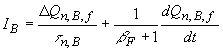

As an example we now apply this charge control model to the abrupt switching of a bipolar transistor. Consider the circuit shown in Figure 5.3.2.(a). As one applies a positive voltage to the base, the base-emitter junction will become forward biased so that the collector current will start to rise. The input is then connected to a negative supply voltage, VR. This reverses the base current and the base-emitter junction capacitance is discharged. After this transient, the transistor is eventually turned off and the collector current reduces back to zero. A full analysis would require solving the charge control model equations simultaneously, while adding the external circuit equations. Such approach requires numeric simulation tools.
To simplify this analysis and provide insight, we now assume that the base current is constant before and after switching. This approximation is very good under forward bias since the base-emitter voltage is almost constant. Under reverse bias, the base current will vary as the base-emitter voltage varies, but conceivably one could design a circuit that does provide a constant reverse current.
The turn-on of the BJT consists of an initial delay time, td,1, during which the base-emitter junction capacitance is charged. This delay is followed by the increase of the collector current, quantified by the rise time, trise. This rise time is obtained by applying the charge control equation for the base current, while applying a base current IBB with the voltage source VBB:


If the device does not reach saturation, the charge reaches its steady state value with a time constant tr,B, which equals the base transit time of the BJT. The corresponding collector current will be proportional to the excess minority carrier charge until the device reaches saturation or:

A larger base voltage, VBB, will therefore result in a larger charging current, IBB, which in turn decreases the rise time and causes the BJT to saturate more quickly. There also will be more excess minority carrier charge stored in the base region after the BJT is turned on. The rise time, trise, is then obtained by finding the time when the saturation current is reached or:

While switching back to the negative power supply, VR, the base current is reversed. As long as significant charge is still stored in the base region, the collector current will continue to exist. Only after this excess charge is removed, will the base-emitter junction capacitor be discharged and the BJT be turned off. The removal of the excess charge can take a significant delay time labeled as td,2 on the figure. Again we can calculate the time evolution of the excess charge and calculate the collector current from it. To first order the delay time, td,2, equals:

This delay time can be significantly larger than the rise time trise. Also note that a higher base turn-on current IBB results in a larger turn-off delay as more minority carrier charge is stored in the base.
The actual fall time, tf, depends on the remaining storage charge at the onset of saturation as well as the charge stored by the base-emitter junction capacitance.

Switching behavior of a BJT: a) bias circuit used to explain the switching behavior. b) Applied voltage and resulting collector current.
No hay comentarios:
Publicar un comentario