domingo, 30 de mayo de 2010


The charge control model of a bipolar transistor is an extension of the charge control model of a p-n diode. Assuming the “short” diode model to be valid, one can express the device currents as a function of the charges in each region, divided by the corresponding transit or lifetime. In the general case one considers the forward bias charges as well as the reverse bias charges. This results in:


Transistor

A transistor is a semiconductor device used to amplify and switch electronic signals. It is made of a solid piece of semiconductor material, with at least three terminals for connection to an external circuit. A voltage or current applied to one pair of the transistor's terminals changes the current flowing through another pair of terminals. Because the controlled (output) power can be much more than the controlling (input) power, the transistor provides amplification of a signal. Today, some transistors are packaged individually, but many more are found embedded in integrated circuits.
The transistor is the fundamental building block of modern electronic devices, and its presence is ubiquitous in modern electronic systems. Following its release in the early 1950s the transistor revolutionised the field of electronics, and paved the way for smaller and cheaper radios, calculators, and computers, amongst other things.


History

Physicist Julius Edgar Lilienfeld filed the first patent for a transistor in Canada in 1925, describing a device similar to a Field Effect Transistor or "FET".However, Lilienfeld did not publish any research articles about his devices,[citation needed] nor did his patent cite any examples of devices actually constructed. In 1934, German inventor Oskar Heil patented a similar device.
In 1947, John Bardeen and Walter Brattain at AT&T's Bell Labs in the United States observed that when electrical contacts were applied to a crystal of germanium, the output power was larger than the input. Solid State Physics Group leader William Shockley saw the potential in this, and over the next few months worked to greatly expand the knowledge of semiconductors, and thus could be described as the "father of the transistor". The term was coined by John R. Pierce. According to physicist/historian Robert Arns, legal papers from the Bell Labs patent show that William Shockley and Gerald Pearson had built operational versions from Lilienfeld's patents, yet they never referenced this work in any of their later research papers or historical articles.
The first silicon transistor was produced by Texas Instruments in 1954. This was the work of Gordon Teal, an expert in growing crystals of high purity, who had previously worked at Bell Labs.The first MOS transistor actually built was by Kahng and Atalla at Bell Labs in 1960.

Importance
The transistor is the key active component in practically all modern electronics, and is considered by many to be one of the greatest inventions of the twentieth century.[Its importance in today's society rests on its ability to be mass produced using a highly automated process (semiconductor device fabrication) that achieves astonishingly low per-transistor costs.
Although several companies each produce over a billion individually-packaged (known as discrete) transistors every year, the vast majority of transistors now produced are in integrated circuits (often shortened to IC, microchips or simply chips), along with diodes, resistors, capacitors and other electronic components, to produce complete electronic circuits. A logic gate consists of up to about twenty transistors whereas an advanced microprocessor, as of 2009, can use as many as 2.3 billion transistors (MOSFETs)."About 60 million transistors were built this year [2002] ... for [each] man, woman, and child on Earth."
The transistor's low cost, flexibility, and reliability have made it a ubiquitous device. Transistorized mechatronic circuits have replaced electromechanical devices in controlling appliances and machinery. It is often easier and cheaper to use a standard microcontroller and write a computer program to carry out a control function than to design an equivalent mechanical control function.
Usage
The bipolar junction transistor, or BJT, was the most commonly used transistor in the 1960s and 70s. Even after MOSFETs became widely available, the BJT remained the transistor of choice for many analog circuits such as simple amplifiers because of their greater linearity and ease of manufacture. Desirable properties of MOSFETs, such as their utility in low-power devices, usually in the CMOS configuration, allowed them to capture nearly all market share for digital circuits; more recently MOSFETs have captured most analog and power applications as well, including modern clocked analog circuits, voltage regulators, amplifiers, power transmitters, motor drivers, etc.

Comparison with vacuum tubes

Prior to the development of transistors, vacuum (electron) tubes (or in the UK "thermionic valves" or just "valves") were the main active components in electronic equipment.
Advantages
The key advantages that have allowed transistors to replace their vacuum tube predecessors in most applications are
Small size and minimal weight, allowing the development of miniaturized electronic devices.
Highly automated manufacturing processes, resulting in low per-unit cost.
Lower possible operating voltages, making transistors suitable for small, battery-powered applications.
No warm-up period for cathode heaters required after power application.
Lower power dissipation and generally greater energy efficiency.
Higher reliability and greater physical ruggedness.
Extremely long life. Some transistorized devices have been in service for more than 30 years.
Complementary devices available, facilitating the design of complementary-symmetry circuits, something not possible with vacuum tubes.
Insensitivity to mechanical shock and vibration, thus avoiding the problem of microphonics in audio applications.
Limitations
Silicon transistors do not operate at voltages higher than about 1,000 volts (SiC devices can be operated as high as 3,000 volts). In contrast, electron tubes have been developed that can be operated at tens of thousands of volts.
High power, high frequency operation, such as that used in over-the-air television broadcasting, is better achieved in electron tubes due to improved electron mobility in a vacuum.
Silicon transistors are much more sensitive than electron tubes to an electromagnetic pulse generated by a high-altitude nuclear explosion.

Types
Transistors are categorized by
Semiconductor material: germanium, silicon, gallium arsenide, silicon carbide, etc.
Structure: BJT, JFET, IGFET (MOSFET), IGBT, "other types"
Polarity: NPN, PNP (BJTs); N-channel, P-channel (FETs)
Maximum power rating: low, medium, high
Maximum operating frequency: low, medium, high, radio frequency (RF), microwave (The maximum effective frequency of a transistor is denoted by the term fT, an abbreviation for "frequency of transition". The frequency of transition is the frequency at which the transistor yields unity gain).
Application: switch, general purpose, audio, high voltage, super-beta, matched pair
Physical packaging: through hole metal, through hole plastic, surface mount, ball grid array, power modules
Amplification factor hfe (transistor beta)
Thus, a particular transistor may be described as silicon, surface mount, BJT, NPN, low power, high frequency switch.


Breakdown mechanisms

Temperature dependent effects in bipolar transistors

The temperature dependence of bipolar transistors depends on a multitude of parameters affecting the bipolar transistor characteristics in different ways.

First we will discuss the temperature dependence of the current gain. Since the current gain depends on both the emitter efficiency and base transport factor, we will discuss these separately.

The emitter efficiency depends on the ratio of the carrier density, diffusion constant and width of the emitter and base. As a result, it is not expected to be very temperature dependent. The carrier densities are linked to the doping densities. Barring incomplete ionization, which can be very temperature dependent, the carrier densities are independent of temperature as long as the intrinsic carrier density does not exceed the doping density in either region. The width is very unlikely to be temperature dependent and therefore also the ratio of the emitter and base width. The ratio of the mobility is expected to be somewhat temperature dependent due to the different temperature dependence of the mobility in n-type and p-type material.

The base transport is more likely to be temperature dependent since it depends on the product of the diffusion constant and carrier lifetime. The diffusion constant in turn equals the product of the thermal voltage and the minority carrier mobility in the base. The recombination lifetime depends on the thermal velocity. The result is therefore moderately dependent on temperature. Typically the base transport reduces with temperature, primarily because the mobility and recombination lifetime are reduced with increasing temperature. Occasionally the transport factor initially increases with temperature, but then reduces again.

Breakdown mechanisms in BJTs

The breakdown mechanisms of BJTs are similar to that of p-n junctions. Since the base-collector junction is reversed biased, it is this junction where breakdown typically occurs. Just like for a p-n junction the breakdown mechanism can be due to either avalanche multiplication as well as tunneling. However, the collector doping in power devices tends to be low-doped either to ensure a large enough breakdown voltage – also called blocking voltage – or to provide a high Early voltage. The collector doping in microwave BJTs is typically higher than that of power devices, yet based on the trade-off between having a short transit time through the base-collector depletion region and having a low base-collector capacitance. As a result, one finds that the collector doping density rarely exceeds 1018 cm-3 and tunneling does not occur.

Instead, breakdown is dominated by avalanche multiplication. The large electric field in the base-collector depletion region causes carrier multiplication due to impact ionization. Just like in a p-n diode, this breakdown is not destructive. However, the high voltage and rapidly increasing current does cause large heat dissipation in the device, which can cause permanent damage to the semiconductor or the contacts.

The breakdown voltage of a BJT also depends on the chosen circuit configuration: In a common base mode (i.e. operation where the base is grounded and forms the common electrode between the emitter-base input and collector-base output of the device) the breakdown resembles that of a p-n diode. In a common emitter mode (i.e. operation where the emitter is grounded and forms the common electrode between the base-emitter input and the collector-emitter output of the device) the transistor action further influences the I-V characteristics and breakdown voltage. Base width modulation was described in section 5.4.1 to result in an increase in the collector current with increased collector-emitter voltage. In the extreme case of punchthrough where the base is completely depleted, an even larger increase is observed be it nowhere as abrupt as in the case of avalanche breakdown. Avalanche breakdown of the base-collector junction is further influenced by transistor action in common-emitter mode of operation, since the holes generated by impact ionization are pulled back into the base region which results in an additional base current. This additional base current causes an even larger additional flow of electrons through the base and into the collector due to the current gain of the BJT. This larger flow of electrons in the base-collector junction causes an even larger generation of electron-hole pairs.

To further analyze this effect quantitatively we first write the total collector current, IC, in response to an applied base current, IB:


Where the term (M - 1) IC was added to the base current to include the holes generated due to impact ionization. This equation can be rearranged to yield:


The collector current will therefore approach infinity as the denominator approaches zero. From this equation and combining with equation one finds that the common emitter breakdown voltage equals:


The common emitter breakdown voltage as characterized by the open base breakdown voltage, VBCEO, is therefore significantly less than the open emitter breakdown voltage, VBCBO.


Comparison of BJT breakdown in common emitter mode (left curve) versus breakdown in common base mode (right curve) for a BJT with VBCBO = 1000V and b = 100

Specification of Transistor Frequency Response

Basic BJT Amplifier Configurations
There are plenty of texts around on basic electronics, so this is a very brief look at the three basic ways in which a bipolar junction transistor (BJT) can be used. In each case, one terminal is common to both the input and output signal. All the circuits shown here are without bias circuits and power supplies for clarity.

Common Emitter Configuration

Here the emitter terminal is common to both the input and output signal. The arrangement is the same for a PNP transistor. Used in this way the transistor has the advantages of a medium input impedance, medium output impedance, high voltage gain and high current gain.

Common Base Configuration

Here the base is the common terminal. Used frequently for RF applications, this stage has the following properties. Low input impedance, high output impedance, unity (or less) current gain and high voltage gain.

Common Collector Configuration
This last configuration is also more commonly known as the emitter follower. This is because the input signal applied at the base is "followed" quite closely at the emitter with a voltage gain close to unity. The properties are a high input impedance, a very low output impedance, a unity (or less) voltage gain and a high current gain. This circuit is also used extensively as a "buffer" converting impedances or for feeding or driving long cables or low impedance loads.

Frequency response
Frequency response is the measure of any system's output spectrum in response to an input signal. In the audible range it is usually referred to in connection with electronic amplifiers, microphones and loudspeakers. Radio spectrum frequency response can refer to measurements of coaxial cables, category cables, video switchers and wireless communications devices. Subsonic frequency response measurements can include earthquakes and electroencephalography (brain waves).
Frequency response requirements differ depending on the application. In high fidelity audio, an amplifier requires a frequency response of at least 20–20,000 Hz, with a tolerance as tight as ±0.1 dB in the mid-range frequencies around 1000 Hz, however, in telephony, a frequency response of 400–4,000 Hz, with a tolerance of ±1 dB is sufficient for intelligibility of speech.
Frequency response curves are often used to indicate the accuracy of electronic components or systems. When a system or component reproduces all desired input signals with no emphasis or attenuation of a particular frequency band, the system or component is said to be "flat", or to have a flat frequency response curve.

The frequency response is typically characterized by the magnitude of the system's response, measured in decibels (dB), and the phase, measured in radians, versus frequency. The frequency response of a system can be measured by applying a test signal, for example:
applying an impulse to the system and measuring its response (see impulse response)
sweeping a constant-amplitude pure tone through the bandwidth of interest and measuring the output level and phase shift relative to the input
applying a signal with a wide frequency spectrum (for example digitally-generated maximum length sequence noise, or analog filtered white noise equivalent, like pink noise), and calculating the impulse response by deconvolution of this input signal and the output signal of the system.
These typical response measurements can be plotted in two ways: by plotting the magnitude and phase measurements to obtain a Bode plot or by plotting the imaginary part of the frequency response against the real part of the frequency response to obtain a Nyquist plot.
Once a frequency response has been measured (e.g., as an impulse response), providing the system is linear and time-invariant, its characteristic can be approximated with arbitrary accuracy by a digital filter. Similarly, if a system is demonstrated to have a poor frequency response, a digital or analog filter can be applied to the signals prior to their reproduction to compensate for these deficiencies.
Frequency response measurements can be used directly to quantify system performance and design control systems. However, frequency response analysis is not suggested if the system has slow dynamics

Amplifier Frequency Response
The essential purpose of an amplifier is to accept an input signal and provide an enhanced copy of that
signal as an output. However there is a fundamental relationship between signal frequency and gain such
that a given gain cannot be maintained over an arbitrarily large frequency range. Physically it takes time for
electric charge in a device to redistribute itself in response to a control signal, and so the response of a
device to a control signal inevitably becomes jumbled for very fast signal changes. This is an ultimate limit
to circuit response; degradation of the response may begin at lower signal frequencies because of delays
associated with other circuit components. Circuit components can introduce degradation of the frequency
response of a circuit at low frequencies as well as high, as will be seen.

In general the frequency response of an electronic circuit, e.g., the
transfer gain of the circuit, has the general appearance illustrated.
There is a ‘mid-band’ range of operation for which the gain is
substantially independent of frequency, bounded by ‘high’ and
‘low’ frequency ranges in which the gain is degraded. An
amplifier is ‘wide-band’ if the ratio of a frequency measuring the
onset of the high-frequency degradation to a corresponding
frequency for low frequency degradation is relatively large. A basic audio amplifier, for example, has a
substantially ‘flat’ response extending from about 100 Hz to roughly 10KHz. ‘Narrow-band’ amplifiers,
used for more specialized purposes, approximate selective amplification at a single frequency. Our basic
interest here is in wide-band amplifiers.
To simplify consideration of the frequency response of wide-band amplifiers analysis generally is
separated into three frequency ranges. The argument used to justify this separation is that those circuit
components associated with low-frequency degradation have by definition lost significant influence on the
response in mid-band, and supposing a monotonic behavior have no influence on the high-frequency
response. The converse argument removes the influence at low frequencies of those components affecting
the high frequency response. And, of course, in mid-band by definition neither of these sets of
components influences the response significantly. The mid-band range is the one assumed in previous
work, for example by neglecting the influence of coupling and bypass capacitors.
Initially we assume that frequency constraints are associated with circuit components o the r than the active
devices. Taking intrinsic device limitations into account is done later as an extension of the basic
procedures.

High Frequency Compensation:
Video Amplifiers
A video amplifier is used to amplify video from TVs, cameras, computer graphic devices, etc. Aside from having sufficient bandwidth and the ability to drive long cables: they cannot invert the signal's polarity; if they did: unless you were using an even number of amplifiers in cascade, the image would end up a negative. If you wanted a gain stage, but didn't want the signal to be inverted, you would drive the emitter instead of the base. This works, but as you might imagine, the input impedance is quite low. So by using what we learned about emitter followers back in chapter 219, we can "transform impedances," and now the noninverting video amplifier looks better.

Bandwidth of an Amplifier
Most amplifiers have relatively constant gain over a certain range (band) of frequencies, this is called the bandwidth (BW) of the amplifier.

As the frequency response curve shows, the gain of an amplifier remains relatively constant across a band of frequencies.
When the operating frequency starts to go outside this frequency range, the gain begins to drop off.
Two frequencies of interest, fC1 and fC2, are identified as the lower and upper cutoff frequencies.
The Bandwidth is found as: BW = fC2 – fC1
The operating frequency of an amplifier is equal to the geometric center frequency fo,
fo = √(fC1 fC2 )
Notice that the ration of fo to fC1 equals the ratio of fC2 to fo , this is:
fo / fC1 = fC2 / fo
Therefore we also have that:
fC1 = fo2 / fC2 ; fC2 = fo2 / fC1

Regions of operation

Active-mode NPN transistors in circuits

The diagram opposite is a schematic representation of an NPN transistor connected to two voltage sources. To make the transistor conduct appreciable current (on the order of 1 mA) from C to E, VBE must be above a minimum value sometimes referred to as the cut-in voltage. The cut-in voltage is usually about 600 mV for silicon BJTs at room temperature but can be different depending on the type of transistor and its biasing. This applied voltage causes the lower P-N junction to 'turn-on' allowing a flow of electrons from the emitter into the base. In active mode, the electric field existing between base and collector (caused by VCE) will cause the majority of these electrons to cross the upper P-N junction into the collector to form the collector current IC. The remainder of the electrons recombine with holes, the majority carriers in the base, making a current through the base connection to form the base current, IB. As shown in the diagram, the emitter current, IE, is the total transistor current, which is the sum of the other terminal currents (i.e., ).
In the diagram, the arrows representing current point in the direction of conventional current – the flow of electrons is in the opposite direction of the arrows because electrons carry negative electric charge. In active mode, the ratio of the collector current to the base current is called the DC current gain. This gain is usually 100 or more, but robust circuit designs do not depend on the exact value (for example see op-amp). The value of this gain for DC signals is referred to as hFE, and the value of this gain for AC signals is referred to as hfe. However, when there is no particular frequency range of interest, the symbol β is used[citation needed].
It should also be noted that the emitter current is related to VBE exponentially. At room temperature, an increase in VBE by approximately 60 mV increases the emitter current by a factor of 10. Because the base current is approximately proportional to the collector and emitter currents, they vary in the same way.


Active-mode PNP transistors in circuits
The diagram opposite is a schematic representation of a PNP transistor connected to two voltage sources. To make the transistor conduct appreciable current (on the order of 1 mA) from E to C, VEB must be above a minimum value sometimes referred to as the cut-in voltage. The cut-in voltage is usually about 600 mV for silicon BJTs at room temperature but can be different depending on the type of transistor and its biasing. This applied voltage causes the upper P-N junction to 'turn-on' allowing a flow of holes from the emitter into the base. In active mode, the electric field existing between the emitter and the collector (caused by VCE) causes the majority of these holes to cross the lower P-N junction into the collector to form the collector current IC. The remainder of the holes recombine with electrons, the majority carriers in the base, making a current through the base connection to form the base current, IB. As shown in the diagram, the emitter current, IE, is the total transistor current, which is the sum of the other terminal currents (i.e., ).
In the diagram, the arrows representing current point in the direction of conventional current – the flow of holes is in the same direction of the arrows because holes carry positive electric charge. In active mode, the ratio of the collector current to the base current is called the DC current gain. This gain is usually 100 or more, but robust circuit designs do not depend on the exact value. The value of this gain for DC signals is referred to as hFE, and the value of this gain for AC signals is referred to as hfe. However, when there is no particular frequency range of interest, the symbol β is used[citation needed].
It should also be noted that the emitter current is related to VEB exponentially. At room temperature, an increase in VEB by approximately 60 mV increases the emitter current by a factor of 10. Because the base current is approximately proportional to the collector and emitter currents, they vary in the same way.


History
The bipolar point-contact transistor was invented in December 1947 at the Bell Telephone Laboratories by John Bardeen and Walter Brattain under the direction of William Shockley. The junction version known as the bipolar junction transistor, invented by Shockley in 1948, enjoyed three decades as the device of choice in the design of discrete and integrated circuits. Nowadays, the use of the BJT has declined in favour of CMOS technology in the design of digital integrated circuits.

Regions of operation
Bipolar transistors have five distinct regions of operation, defined mostly by applied bias:
Forward-active (or simply, active): The base–emitter junction is forward biased and the base–collector junction is reverse biased. Most bipolar transistors are designed to afford the greatest common-emitter current gain, βF, in forward-active mode. If this is the case, the collector–emitter current is approximately proportional to the base current, but many times larger, for small base current variations.
Reverse-active (or inverse-active or inverted): By reversing the biasing conditions of the forward-active region, a bipolar transistor goes into reverse-active mode. In this mode, the emitter and collector regions switch roles. Because most BJTs are designed to maximize current gain in forward-active mode, the βF in inverted mode is several (2–3 for the ordinary germanium transistor) times smaller. This transistor mode is seldom used, usually being considered only for failsafe conditions and some types of bipolar logic. The reverse bias breakdown voltage to the base may be an order of magnitude lower in this region.
Saturation: With both junctions forward-biased, a BJT is in saturation mode and facilitates high current conduction from the emitter to the collector. This mode corresponds to a logical "on", or a closed switch.
Cutoff: In cutoff, biasing conditions opposite of saturation (both junctions reverse biased) are present. There is very little current flow, which corresponds to a logical "off", or an open switch.
Avalanche breakdown region

Although these regions are well defined for sufficiently large applied voltage, they overlap somewhat for small (less than a few hundred millivolts) biases. For example, in the typical grounded-emitter configuration of an NPN BJT used as a pulldown switch in digital logic, the "off" state never involves a reverse-biased junction because the base voltage never goes below ground; nevertheless the forward bias is close enough to zero that essentially no current flows, so this end of the forward active region can be regarded as the cutoff region.

To understand the three regions of operation of the transistor, consider the circuit below:

The first region is called “cutoff”. This is the case where the transistor is essentially inactive.
In cutoff, the following behavior is noted:
* Ib = 0 (no base current)
* Ic = 0 (no collector current)
* Vbe <>

Whenever we observe the terminals of a BJT and see that the emitter-base junction is not at
least 0.6-0.7 volts, the transistor is in the cutoff region. In cutoff, the transistor appears as an
open circuit between the collector and emitter terminals. In the circuit above, this implies Vout
is equal to 10 volts.
The second region is called “saturation”. This is where the base current has increased well
beyond the point that the emitter-base junction is forward biased. In fact, the base current has
increased beyond the point where it can cause the collector current flow to increase. In saturation,
the transistor appears as a near short circuit between the collector and emitter terminals.
In the circuit above, this implies Vout is almost 0 volts, but actually about 0.2 volts.
In saturation, the following behavior is noted:
* Vce <= 0.2V. This is known as the saturation voltage, or Vce(sat)
* Ib > 0, and Ic > 0
* Vbe >= 0.7V
Using the two states of cutoff and saturation, the transistor may be used as a switch. The collector
and emitter form the switch terminals and the base is the switch handle. In other words,
the small base current can be made to control a much larger current between the collector and
emitter. For example, the circuit above can be modified to control an electric motor. The motor
would replace the collector resistor and transistor would act as a switch. See the drawing
below.

When high current motors are switched on and off, mechanical switch contacts can eventually
wear out causing the switch to fail., The BJT can operate as a switch however that has no mechanism that causes it wear out. When it is saturated, the bottom terminal of the motor is
essentially connected to ground. When cutoff, the bottom end of the motor is seemingly not
connected to anything. Used in this manner, the switch only has to handle 1/100 of the motor
current, greatly increasing its life.
The final region of operation of the BJT is the “forward active” region. It is in this region that
the transistor can act as a fairly linear amplifier. In this region, we see that:
* 0.2 <>
* Ib > 0 and Ic > 0
* Vbe >= 0.7V
Thus the transistor is on and the collector to emitter voltage is somewhere between the cutoff
and saturated states. In this state, the transistor is able to amplify small variations in the voltage
present on the base. The output is extracted at the collector. In the forward active state, the
collector current is proportional to the base current by a constant multiplier called “beta”,
denoted by the symbol b. Thus in the forward active region we will also observe that:
* Ic = b*Ib
When high current motors are switched on and off, mechanical switch contacts can eventually
wear out causing the switch to fail., The BJT can operate as a switch however that has no
mechanism that causes it wear out. When it is saturated, the bottom terminal of the motor is
essentially connected to ground. When cutoff, the bottom end of the motor is seemingly not
connected to anything. Used in this manner, the switch only has to handle 1/100 of the motor
current, greatly increasing its life.
The final region of operation of the BJT is the “forward active” region. It is in this region that
the transistor can act as a fairly linear amplifier. In this region, we see that:
* 0.2 <>
* Ib > 0 and Ic > 0
* Vbe >= 0.7V
Thus the transistor is on and the collector to emitter voltage is somewhere between the cutoff
and saturated states. In this state, the transistor is able to amplify small variations in the voltage
present on the base. The output is extracted at the collector. In the forward active state, the
collector current is proportional to the base current by a constant multiplier called “beta”,
denoted by the symbol b. Thus in the forward active region we will also observe that:
* Ic = b*Ib


Characteristics in the Forward-Active Region

The ideal transistor model is based on the ideal p-n diode model and provides a first-order calculation of the dc parameters of a bipolar junction transistor. To further simplify this model, we will assume that all quasi-neutral regions in the device are much smaller than the minority-carrier diffusion lengths in these regions, so that the "short" diode expressions apply. The use of the ideal p-n diode model implies that no recombination within the depletion regions is taken into account.

The discussion of the ideal transistor starts with a discussion of the forward active mode of operation, followed by a general description of the four different bias modes, the corresponding Ebers-Moll model and a calculation of the collector-emitter voltage when the device is biased in saturation.

Forward active mode of operation
The forward active mode is obtained by forward-biasing the base-emitter junction. In addition we eliminate the base-collector junction current by setting VBC = 0. The minority-carrier distribution in the quasi-neutral regions of the bipolar transistor, is used to analyze this situation in more detail.


Minority-carrier distribution in the quasi-neutral regions of a bipolar transistor (a) Forward active bias mode. (b) Saturation model

The values of the minority carrier densities at the edges of the depletion regions are indicated on the Figure. The carrier densities vary linearly between the boundary values as expected when using the assumption that no significant recombination takes place in the quasi-neutral regions. The minority carrier densities on both sides of the base-collector depletion region equal the thermal equilibrium values since VBC was set to zero. While this boundary condition is mathematically equivalent to that of an ideal contact, there is an important difference. The minority carriers arriving at x = wB - xp,BC do not recombine. Instead, they drift through the base-collector depletion region and end up as majority carriers in the collector region.

The emitter current due to electrons and holes are obtained using the "short" diode expressions, yielding:


which for a "short" diode becomes:


And the emitter current due to electrons, IE,n, simplifies to:


where tr is the average time the minority carriers spend in the base layer, i.e. the transit time. The emitter current therefore equals the excess minority carrier charge present in the base region, divided by the time this charge spends in the base.

A combination of equations yields the transit time as a function of the quasi-neutral layer width, wB', and the electron diffusion constant in the base, Dn,B.


We now turn our attention to the recombination current in the quasi-neutral base and obtain it from the continuity equation


By applying it to the quasi-neutral base region and assuming steady state conditions


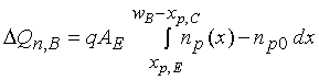
which in turn can be written as a function of the excess minority carrier charge, DQn,B


Next, we need to find the emitter efficiency and base transport fact


It is typically the emitter efficiency, which limits the current gain in transistors made of silicon or germanium. The long minority-carrier lifetime and the long diffusion lengths in those materials justify the exclusion of recombination in the base or the depletion layer. The resulting current gain, under such conditions, is:

From this equation, we conclude that the current gain can be larger than one if the emitter doping is much larger than the base doping. A typical current gain for a silicon bipolar transistor is 50 - 150.

This expression is only valid if the base transport factor is very close to one, since it was derived using the “short-diode” carrier distribution. This base transport factor can also be expressed in function of the diffusion length in the base:

Early effect

The Early effect is the variation in the width of the base in a BJT due to a variation in the applied base-to-collector voltage, named after its discoverer James M. Early. A greater reverse bias across the collector–base junction, for example, increases the collector–base depletion width, decreasing the width of the charge neutral portion of the base.

In the Figure the neutral base width is dark blue, and the depleted base regions are light blue. The neutral emitter and collector regions are dark red and the depleted regions pink. Under increased collector–base reverse bias, the lower panel of Figure shows a widening of the depletion region in the base and the associated narrowing of the neutral base region.
The collector depletion region also increases under reverse bias, more than does that of the base, because the collector is less heavily doped. The principle governing these two widths is charge neutrality. The emitter–base junction is unchanged because the emitter–base voltage is the same.
Top: pnp base width for low collector–base reverse bias; Bottom: narrower pnp base width for large collector–base reverse bias. Light colors are depleted regions.
The collector depletion region also increases under reverse bias, more than does that of the base, because the collector is less heavily doped. The principle governing these two widths is charge neutrality. The emitter–base junction is unchanged because the emitter–base voltage is the same.
Base-narrowing has two consequences that affect the current:
There is a lesser chance for recombination within the "smaller" base region.
The charge gradient is increased across the base, and consequently, the current of minority carriers injected across the emitter junction increases.
Both these factors increase the collector or "output" current of the transistor with an increase in the collector voltage. This increased current is shown in Figure 2. Tangents to the characteristics at large voltages extrapolate backward to intercept the voltage axis at a voltage called the Early voltage, often denoted by the symbol VA.

The Early voltage as seen in the output-characteristic plot of a BJT

Large-signal model
In the forward active region the Early effect modifies the collector current (IC) and the forward common-emitter current gain (βF), as typically described by the following equations


Where
-VCE is the collector–emitter voltage
-VT is the thermal voltage kT / q; see thermal voltage: role in semiconductor physics
-VA is the Early voltage (typically 15 V to 150 V; smaller for smaller devices)
-βF0 is forward common-emitter current gain at zero bias.
Some models base the collector current correction factor on the collector–base voltage VCB (as described in base-width modulation) instead of the collector–emitter voltage VCE.Using VCB may be more physically plausible, in agreement with the physical origin of the effect, which is a widening of the collector–base depletion layer that depends on VCB. Computer models such as those used in SPICE use the collector–base voltage VCB.

Small-signal model
The Early effect can be accounted for in small-signal circuit models (such as the hybrid-pi model) as a resistor defined as


in parallel with the collector–emitter junction of the transistor. This resistor can thus account for the finite output resistance of a simple current mirror or an actively loaded common-emitter amplifier.
In keeping with the model used in SPICE and as discussed above using VCB the resistance becomes:


which almost agrees with the textbook result. In either formulation, rO varies with DC reverse bias VCB, as is observed in practice.
In the MOSFET the output resistance is given in Shichman–Hodges model (accurate for very old technology) as:

where VDS = drain-to-source voltage, ID = drain current and λ = channel-length modulation parameter, usually taken as inversely proportional to channel length L. Because of the resemblance to the bipolar result, the terminology "Early effect" often is applied to the MOSFET as well.
A bipolar junction transistor is formed by joining three sections of semiconductors with
alternatively di erent dopings. The middle section (base) is narrow and one of the other two
regions (emitter) is heavily doped. Two variants of BJT are possible: NPN and PNP.

We will focus on NPN BJTs. Operation of a PNP transistor is analogous to that of a NPN transistor except that the role of \majority" charge carries reversed. In NPN transistors, electron flow is dominant while PNP transistors rely mostly on the flow of \holes." Therefore, to zeroth order, NPN and PNP transistors behave similarly except the sign of current and voltages are reversed. i.e., PNP = -NPN. In practice, NPN transistors are much more popular than PNP transistors because electrons move faster in a semiconductor. As a results, a NPN transistor has a faster response time compared to a PNP transistor.

At the first glance, a BJT looks like 2 diodes placed back to back. Indeed this is the case if we apply voltage to only two of the three terminals, letting the third terminal
oat. This is also the way that we check if a transistor is working: use an ohm-meter to ensure both diodes are in working conditions. (One should also check the resistance between CE terminals and read a vary high resistance as one may have a burn through the base connecting collector and emitter.)

The behavior of the BJT is di erent, however, when voltage sources are attached to both BE and CE terminals. The BE junction acts like a diode. When this junction is forward biased, electrons
ow from emitter to the base (and a small current of holes from base to emitter). The base region is narrow and when a voltage is applied between collector and emitter, most of the electrons that were flowing from emitter to base, cross the narrow base region and are collected at the collector region. So while the BC junction is reversed biased, a large current can flow through that region and BC junction does not act as a diode. The amount of the current that crosses from emitter to collector region depends strongly on the voltage applied to the BE junction, vBE. (It also depends weakly on voltage applied between collector and emitter, vCE.) As such, small changes in vBE or iB controls a much larger collector current iC. Note that the transistor does not generate iC. It acts as a valve ncontrolling the current that can flow through it. The source of current (and power) is the power supply that feeds the CE terminals.

Several "models" available for a BJT. These are typically divided into two general categories:
"large-signal" models that apply to the entire range of values of current and voltages, and "small-signal" models that apply to AC signals with small amplitudes. \Low-frequency" and"high-frequency" models also exist (high-frequency models account for capacitance of each junction). Obviously, the simpler the model, the easier the circuit calculations are. More complex models describe the behavior of a BJT more accurately but analytical calculations become dificult. PSpice program uses a high-frequency, Eber-Mos large-signal model which is a quite accurate representation of BJT. For analytical calculations here, we will discuss a simple low-frequency, large-signal model (below) and a low-frequency, small-signal model in the context of BJT amplifiers later.

Large signal model (Charge control model)
The charge control model of a bipolar transistor is an extension of the charge control model of a p-n diode. Assuming the “short” diode model to be valid, one can express the device currents as a function of the charges in each region, divided by the corresponding transit or lifetime. In the general case one considers the forward bias charges as well as the reverse bias charges. This results in: